The article below discuss using CTF instead of floating gate to create 3D flash memory with up to 1T SSD product next year.
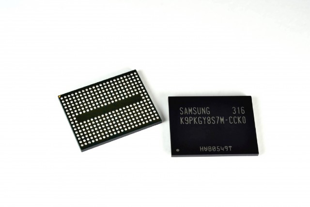
" new V-NAND is manufactured at a 10nm process size, and it starts at a density of 128Gb per NAND chip. The NAND chips are constructed in layers, stacking up to 24 individual NAND cells on top of each other...
Samsung is claiming that at minimum, the CTF-based V-NAND has at least a 2x increase in lifespan over floating gate NAND, and perhaps as high as 10x. Additionally, write performance is doubled over floating gate NAND."
Already in 2006 Samsung discussed CTF memory cell for NAND chips CTF for 40nm 32Gb .
Longer life, higher reliability, more performance—what's not to like?
by Lee Hutchinson - Aug 6 2013, 7:50am PDT
SSD enthusiasts know all about SLC, MLC, and TLC, but there are some new acronyms in SSD town: V-NAND and CTF. Samsung announced in a press release last night that it has begun mass production of "3D Vertical NAND," a type of flash that it claims overcomes the existing limits on the design and production of existing NAND types. When we looked at those limits about a year ago, they seemed pretty significant; Samsung's V-NAND aims to neatly sidestep most of the issues.
Enlarge/ Samsung's 3D Vertical NAND stacks up to 24 NAND elements on top of each other.
The new V-NAND is manufactured at a 10nm process size, and it starts at a density of 128Gb per NAND chip. The NAND chips are constructed in layers, stacking up to 24 individual NAND cells on top of each other. This lets S amsung scale the chip's capacity up without having to add more NAND cells in a series, or "planar scaling," as the traditional "just shrink 'em and add more cells" method is called.
The other acronym, CTF, stands for "Charge Trap Flash." Traditional NAND flash records zeros and ones by storing charge in a set of floating gate transistors, with the presence or absence of charge corresponding to a 0 or a 1 in single-level cell NAND, and the amount of charge corresponding to different multibit values in multi- and triple-level cell NAND (we have an extremely in-depth primer on the inner workings of SSDs if you want more details). However, Samsung's new V-NAND dispenses with floating gate transistors and uses a different method:
Samsung's CTF-based NAND flash architecture, an electric charge is temporarily placed in a holding chamber of the non-conductive layer of flash that is composed of silicon nitride (SiN), instead of using a floating gate to prevent interference between neighboring cells.
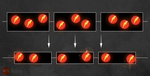
The longevity and reliability problems with standard floating gate transistor-based NAND have a lot to do with the large amounts of power required to perform erasures. Without taking too large a digression, each time a NAND transistor undergoes a program/erase cycle, it retains some additional electrons in its dielectric layer. Eventually, these trapped electrons alter the transistor's resistance to the point that it can no longer be reliably read. The problem grows worse as the NAND cell manufacturing process shrinks—smaller cells become useless at lower levels of retained charge.
Smaller NAND transistor gates means it takes a smaller retained charge to overwhelm the gates' ability to quickly and reliably change state.
Aurich Lawson
The switch from floating gate to Charge Trap Flash appears to negate a lot of these issues. Samsung is claiming that at minimum, the CTF-based V-NAND has at least a 2x increase in lifespan over floating gate NAND, and perhaps as high as 10x. Additionally, write performance is doubled over floating gate NAND.
Samsung predicts that V-NAND will scale up to 1Tb per individual NAND chip. Most SSDs use at least eight NAND chips in parallel, so V-NAND could lead directly to low dollar-per-GB 2.5-inch form factor SSDs of 1TB and beyond—capacities which many Ars commenters have said repeatedly that they desperately want. At that size, concerns over installing an operating system and a few games on a fast SSD and stashing non-speed-critical files on a larger HDD are moot, and most folks can simply use the SSD exclusively without worry. There's no word yet on exactly when a consumer-level SSD filled with V-NAND will become available, but Samsung's vertical integration likely means that the first V-NAND SSD will be a Samsung-branded product with a Samsung-branded SSD controller.


No comments:
Post a Comment